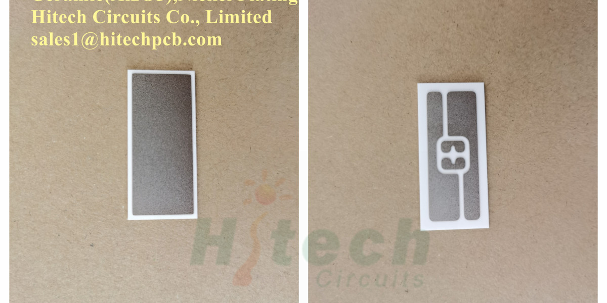
High-Performance Ceramic PCBs from China: Precision, Reliability, and Innovation
In the realm of advanced electronics, where high power density, extreme temperatures, and miniaturization are critical, ceramic PCBs (printed circuit boards) have emerged as a game-changing solution. Manufactured with cutting-edge technology in China, these PCBs combine superior material properties with cost-effective production, making them indispensable for industries pushing the boundaries of performance. Whether for aerospace, automotive, or next-gen telecommunications, ceramic PCBs made in China stand at the forefront of innovation, delivering unmatched quality and value. Pls send PCB files to sales1@hitechpcb.com to get a quote now!
Why Ceramic PCBs?
Ceramic PCBs utilize substrates like alumina (Al₂O₃), aluminum nitride (AlN), or silicon nitride (Si₃N₄), offering unique advantages over traditional FR-4 or metal-core boards:
- Exceptional Thermal Conductivity: Ranging from 24–320 W/m·K (depending on material), ceramic substrates efficiently dissipate heat from high-power components, preventing thermal failure.
- High Electrical Insulation: Withstand voltages up to 15–25 kV/mm, ideal for high-frequency and high-voltage applications.
- Thermal Stability: Operate reliably in extreme temperatures (-55°C to +850°C) without warping or degradation.
- Chemical Resistance: Immune to moisture, acids, and corrosive environments.
- Miniaturization Potential: Enable ultra-thin, high-density designs for compact devices.
China’s Edge in Ceramic PCB Manufacturing
China has solidified its position as a global leader in ceramic PCB production, driven by:
- Advanced Material Expertise
Chinese manufacturers master the synthesis and processing of advanced ceramics (e.g., AlN for ultra-high thermal conductivity), ensuring optimal performance for niche applications. - State-of-the-Art Fabrication Technologies
- Thick-Film & Thin-Film Printing: Precision deposition of conductive traces (Au, Ag, Cu) for high-frequency circuits.
- LTCC/HTCC (Low/High-Temperature Co-Fired Ceramics): Multi-layer designs with embedded components for RF and microwave systems.
- Laser Machining: Micron-level accuracy for intricate circuit patterns and micro-vias.
- Cost-Effective Scalability
Leveraging automated production lines and economies of scale, Chinese suppliers deliver premium ceramic PCBs at competitive prices. - Global Compliance & Certifications
Adherence to ISO, IPC, RoHS, and UL standards ensures compatibility with international markets.
Key Applications of Ceramic PCBs
- Power Electronics
- EV/HEV inverters, IGBT modules, and motor drives.
- Solar power converters and wind turbine control systems.
- LED Lighting
High-power LED arrays for automotive headlights, stadium lighting, and UV sterilization. - Aerospace & Defense
Radar systems, satellite communication modules, and avionics requiring radiation-hardened solutions. - 5G & RF Devices
Base station amplifiers, RF filters, and millimeter-wave circuits for ultra-fast data transmission. - Medical Equipment
Implantable devices, MRI systems, and laser surgical tools demanding biocompatibility and precision. - Industrial Sensors
High-temperature pressure sensors, gas detectors, and IoT edge devices.
Features of Premium Ceramic PCBs from China
- Material Versatility
- Alumina (Al₂O₃): Cost-effective, widely used for LED and power modules.
- Aluminum Nitride (AlN): Ultra-high thermal conductivity (170–320 W/m·K) for high-frequency ICs.
- Silicon Nitride (Si₃N₄): Exceptional mechanical strength for harsh environments.
- Customization Capabilities
- Layer count (1–10+ layers).
- Surface finishes (ENIG, immersion tin, gold plating).
- Thickness (0.25 mm to 2.5 mm).
- Complex shapes and cutouts via laser or CNC machining.
- Superior Signal Integrity
Low dielectric loss and stable impedance control for high-speed digital and RF circuits. - Rigorous Quality Assurance
- Automated Optical Inspection (AOI).
- X-ray testing for layer alignment and via integrity.
- Thermal shock and humidity resistance testing.
Why Partner with Chinese Ceramic PCB Suppliers?
- End-to-End Solutions
From design simulation and prototyping to mass production and certification support. - R&D Collaboration
Work with engineers to optimize thermal management, material selection, and layout for your application. - Fast Turnaround
Prototypes delivered in 5–7 days; bulk orders with flexible MOQs. - Sustainable Practices
Eco-friendly production processes and recyclable material options. - Global Logistics Network
Seamless export to Europe, North America, and Asia with full documentation support.
Conclusion
As industries evolve toward higher efficiency, smaller form factors, and extreme operational demands, ceramic PCBs made in China offer a future-proof solution. Combining advanced material science, precision engineering, and cost competitiveness, Chinese manufacturers are redefining the possibilities for next-generation electronics.
Whether you’re developing cutting-edge 5G infrastructure, electric vehicle systems, or life-saving medical devices, partnering with a trusted Chinese ceramic PCB supplier ensures your products achieve peak performance, reliability, and market success.
https://hitechcircuits.com/pcb-products/ceramic-pcb/


